In what application is gallium arsenide used as a semiconductor material?
AnswerIn microwave circuits
Gallium arsenide is useful at very high frequencies because of its semiconductor properties, so the pool associates it with microwave circuits.
Amateur Extra · correct answers only, in question-pool order.
Gallium arsenide is useful at very high frequencies because of its semiconductor properties, so the pool associates it with microwave circuits.
N-type semiconductor material is doped so electrons are the majority carriers, giving it an excess of free electrons.
Reverse bias pulls majority carriers away from the PN junction, widening the depletion region and greatly reducing current flow.
An impurity that creates holes in a semiconductor crystal is called an acceptor impurity.
The insulated or reverse-biased gate structure of an FET draws very little DC current, so an FET generally has much higher DC input impedance than a bipolar transistor.
Bipolar transistor beta is current gain: the change in collector current divided by the corresponding change in base current.
A silicon NPN transistor that is forward biased on typically has about 0.6 to 0.7 volt from base to emitter.
The alpha cutoff frequency is where grounded-base current gain has fallen to about 0.7 of its low-frequency value.
A depletion-mode FET conducts between source and drain even with zero gate voltage applied.

In Figure E6-1, symbol 4 is the N-channel dual-gate MOSFET.
In Figure E6-1, symbol 1 is the P-channel junction FET.
MOSFET gates are vulnerable to electrostatic overvoltage. Zener diodes connected between the gate and source or drain clamp excessive voltage and protect the gate.
A Zener diode is useful because, in its operating region, it maintains a nearly constant voltage over a range of current.
A Schottky diode has a lower forward voltage drop than a conventional silicon PN-junction diode, reducing conduction loss in rectifier service.
The semiconductor band gap determines the photon energy and therefore the forward-voltage behavior associated with an LED material.
A varactor diode is operated so its junction capacitance varies with applied reverse voltage, making it a voltage-controlled capacitor.
A PIN diode has very low junction capacitance when reverse biased, helping it isolate RF signals effectively in switching applications.
Schottky diodes switch quickly and have useful high-frequency behavior, making them common as VHF/UHF mixers and detectors.
Excessive forward current overheats the diode junction. If the junction temperature becomes too high, the device can fail.
A Schottky barrier diode uses a metal-semiconductor junction rather than a conventional PN junction.
Point-contact diodes are useful at RF because their small junction and low capacitance make them effective detectors.

In Figure E6-2, symbol 6 is the Schottky diode.
A PIN diode's RF resistance can be controlled with forward DC bias current, allowing it to act as a variable RF attenuator.
Comparator hysteresis creates separate switching thresholds for rising and falling inputs, preventing small amounts of noise from repeatedly toggling the output.
When the comparator input crosses its threshold voltage, the comparator changes output state.
Tri-state logic provides three possible output conditions: logic 0, logic 1, and a high-impedance disconnected state.
BiCMOS combines CMOS input characteristics with bipolar output capability, giving high input impedance and low output impedance.
Among the listed digital logic families, CMOS has the lowest power consumption.
CMOS logic thresholds are typically near the middle of the supply range, giving substantial noise margin before an unintended input change is interpreted as a new logic state.
A pull-up or pull-down resistor connects a signal to a supply rail so the line assumes a defined voltage when no active device is driving it.
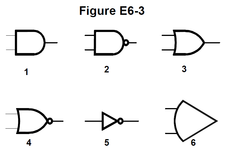
In Figure E6-3, symbol 2 is the NAND gate.
Field-programmable gate arrays are configured using a hardware description language such as VHDL or Verilog.
In Figure E6-3, symbol 4 is the NOR gate.
In Figure E6-3, symbol 5 is the NOT or inverter function.
Piezoelectric materials convert between mechanical stress and electrical voltage: stressing the material generates voltage, and applying voltage causes mechanical deformation.
A quartz crystal is modeled as a series RLC branch in parallel with a shunt capacitance representing the electrodes and stray capacitance.
One side of the piezoelectric effect is mechanical deformation caused by applying an electric voltage.
Laminating magnetic cores into thin layers breaks up circulating eddy-current paths and reduces core power loss.
Ferrite generally has higher permeability than powdered iron, so fewer turns are required to obtain the same inductance.
Core permeability determines how strongly the core supports magnetic flux and therefore has a major effect on inductance.
Among the listed materials, powdered iron has the highest temperature stability of its magnetic characteristics.
Ferrite beads are commonly placed at transistor-amplifier terminals to add loss and impedance at VHF/UHF parasitic frequencies.
A toroidal core forms a closed magnetic path, confining most of the magnetic field within the core material.
A brass core acts as a conductive, nonmagnetic slug that can reduce the inductance of a coil.
An inductor core saturates when magnetic flux becomes excessive and the core can no longer respond proportionally to additional magnetizing force.
Gallium arsenide offers high electron mobility, which supports high-speed device operation at UHF and microwave frequencies.
A DIP, or dual in-line package, is a traditional through-hole IC package with pins inserted through circuit-board holes.
Among the listed materials, gallium nitride supports the highest frequency of MMIC operation.
Most RF MMICs are designed for standard 50-ohm input and output systems.
A noise figure around 0.5 dB is typical of a good low-noise UHF preamplifier.
MMICs are popular because they provide controlled gain, low noise figure, and relatively constant input and output impedance across their specified frequency range.
Microstrip is commonly used to connect MMICs because short controlled-impedance traces can be formed directly on the circuit board.
Many common MMICs receive DC bias through a resistor and/or RF choke connected to the amplifier output lead while RF is coupled separately.
Surface-mount packages have very short leads and compact geometry, so they introduce the least parasitic inductance and capacitance of the listed package types above HF.
The official E6E10 source lists smaller circuit area as one RF advantage of surface-mount technology compared with through-hole construction.
The official E6E10 source lists shorter circuit-board traces as an RF advantage of surface-mount technology.
The official E6E10 source identifies reduced parasitic inductance and capacitance as an RF advantage of surface-mount components.
DIP means dual in-line package: two parallel rows of connecting pins on opposite sides of the package.
Through-hole DIP leads are relatively long, and at UHF those leads introduce too much unwanted inductance and capacitance.
According to the Extra pool, electrons absorb the energy from light falling on a photovoltaic cell, enabling the cell to produce electrical output.
Illumination creates additional charge carriers in photoconductive material, so its resistance decreases.
The most common optoisolator pairs an LED with a phototransistor, transferring a signal optically while maintaining electrical isolation.
The photovoltaic effect is the conversion of light energy into electrical energy.
An optical shaft encoder uses a patterned wheel to interrupt or pass light as the shaft turns, converting rotation into pulses or position information.
Crystalline semiconductor material is commonly used for photoconductive devices because its conductivity changes when light creates charge carriers.
A solid-state relay uses semiconductor devices to perform the switching function of an electromechanical relay without moving contacts.
Optoisolators let a low-voltage control circuit operate a 120 VAC circuit while maintaining electrical isolation between the two sides.
The pool defines photovoltaic efficiency as the relative fraction of incident light converted to current.
Silicon is the most common semiconductor material used in power-generating photovoltaic cells.
A fully illuminated silicon photovoltaic cell produces approximately 0.5 volt open circuit.